- 您现在的位置:买卖IC网 > Sheet目录2006 > LTC2495CUHF#PBF (Linear Technology)IC ADC 16BIT W/PGA 38-QFN
LTC2495
2495fd
I2C INTERFACE
The LTC2495 communicates through an I2C interface. The
I2C interface is a 2-wire, open-drain interface supporting
multiple devices and multiple masters on a single bus. The
connected devices can only pull the data line (SDA) LOW
and can never drive it HIGH. SDA is required to be exter-
nally connected to the supply through a pull-up resistor.
When the data line is not being driven, it is HIGH. Data on
the I2C bus can be transferred at rates up to 100kbits/s in
the standard mode and up to 400kbits/s in the fast mode.
The VCC power should not be removed from the device
when the I2C bus is active to avoid loading the I2C bus
lines through the internal ESD protection diodes.
Each device on the I2C bus is recognized by a unique
address stored in that device and can operate either as a
transmitter or receiver, depending on the function of the
device. In addition to transmitters and receivers, devices
canalsobeconsideredasmastersorslaveswhenperform-
ing data transfers. A master is the device which initiates a
data transfer on the bus and generates the clock signals
to permit that transfer. Devices addressed by the master
are considered a slave.
The LTC2495 can only be addressed as a slave. Once
addressed, it can receive configuration bits (channel
selection, rejection mode, speed mode) or transmit the
last conversion result. The serial clock line, SCL, is always
an input to the LTC2495 and the serial data line SDA is
bidirectional. The device supports the standard mode and
the fast mode for data transfer speeds up to 400kbits/s.
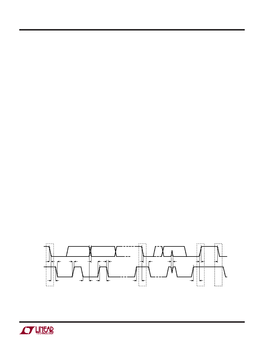
Figure 2 shows the definition of the I2C timing.
The START and STOP Conditions
A START (S) condition is generated by transitioning SDA
from HIGH to LOW while SCL is HIGH. The bus is consid-
ered to be busy after the START condition. When the data
transfer is finished, a STOP (P) condition is generated by
transitioning SDA from LOW to HIGH while SCL is HIGH.
The bus is free after a STOP is generated. START and STOP
conditions are always generated by the master.
When the bus is in use, it stays busy if a repeated START
(Sr)isgeneratedinsteadofaSTOPcondition.Therepeated
START timing is functionally identical to the START and is
used for writing and reading from the device before the
initiation of a new conversion.
Data Transferring
After the START condition, the I2C bus is busy and data
transfer can begin between the master and the addressed
slave. Data is transferred over the bus in groups of nine
bits, one byte followed by one acknowledge (ACK) bit. The
master releases the SDA line during the ninth SCL clock
cycle. The slave device can issue an ACK by pulling SDA
LOW or issue a Not Acknowledge (NACK) by leaving the
SDA line high impedance (the external pull-up resistor will
hold the line HIGH). Change of data only occurs while the
clock line (SCL) is LOW.
Figure 2. Definition of Timing for Fast/Standard Mode Devices on the I2C Bus
applications inForMation
SDA
SCL
S
Sr
P
S
tHD(SDA)
tHD(DAT)
tSU(STA)
tSU(STO)
tSU(DAT)
tLOW
tHD(SDA)
tSP
tBUF
tr
tf
tr
tf
tHIGH
2495 F02
发布紧急采购,3分钟左右您将得到回复。
相关PDF资料
LTC2496IUHF#TRPBF
IC ADC 16BIT DELTA SIG 38-QFN
LTC2498IUHF#TRPBF
IC ADC 24BIT 16CH 38-QFN
LTC2600IUFD#PBF
IC DAC OCTAL R-R 16BIT 20-QFN
LTC2602IMS8#TRPBF
IC DAC 16BIT DUAL R-R VOUT 8MSOP
LTC2604IGN-1#TRPBF
IC DAC 16BIT QUAD R-R OUT 16SSOP
LTC2605IGN-1#TRPBF
IC DAC 16BIT OCT I2C 16-SSOP
LTC2606IDD#TRPBF
IC DAC 16BIT I2C V-OUT 10-DFN
LTC2607IDE#TRPBF
IC DAC 16BIT R-R I2C 12-DFN
相关代理商/技术参数
LTC2495CUHF#TRPBF
功能描述:IC ADC 16BIT W/PGA 38-QFN RoHS:是 类别:集成电路 (IC) >> 数据采集 - 模数转换器 系列:- 标准包装:2,500 系列:- 位数:16 采样率(每秒):15 数据接口:MICROWIRE?,串行,SPI? 转换器数目:1 功率耗散(最大):480µW 电压电源:单电源 工作温度:-40°C ~ 85°C 安装类型:表面贴装 封装/外壳:38-WFQFN 裸露焊盘 供应商设备封装:38-QFN(5x7) 包装:带卷 (TR) 输入数目和类型:16 个单端,双极;8 个差分,双极 配用:DC1011A-C-ND - BOARD DELTA SIGMA ADC LTC2494
LTC2495IUHF#PBF
功能描述:IC ADC 16BIT W/PGA 38-QFN RoHS:是 类别:集成电路 (IC) >> 数据采集 - 模数转换器 系列:- 标准包装:1 系列:microPOWER™ 位数:8 采样率(每秒):1M 数据接口:串行,SPI? 转换器数目:1 功率耗散(最大):- 电压电源:模拟和数字 工作温度:-40°C ~ 125°C 安装类型:表面贴装 封装/外壳:24-VFQFN 裸露焊盘 供应商设备封装:24-VQFN 裸露焊盘(4x4) 包装:Digi-Reel® 输入数目和类型:8 个单端,单极 产品目录页面:892 (CN2011-ZH PDF) 其它名称:296-25851-6
LTC2495IUHF#TRPBF
功能描述:IC ADC 16BIT W/PGA 38-QFN RoHS:是 类别:集成电路 (IC) >> 数据采集 - 模数转换器 系列:- 标准包装:1,000 系列:- 位数:16 采样率(每秒):45k 数据接口:串行 转换器数目:2 功率耗散(最大):315mW 电压电源:模拟和数字 工作温度:0°C ~ 70°C 安装类型:表面贴装 封装/外壳:28-SOIC(0.295",7.50mm 宽) 供应商设备封装:28-SOIC W 包装:带卷 (TR) 输入数目和类型:2 个单端,单极
LTC2496CUHF#PBF
功能描述:IC ADC 16BIT DELTA SIG 38-QFN RoHS:是 类别:集成电路 (IC) >> 数据采集 - 模数转换器 系列:- 标准包装:1 系列:microPOWER™ 位数:8 采样率(每秒):1M 数据接口:串行,SPI? 转换器数目:1 功率耗散(最大):- 电压电源:模拟和数字 工作温度:-40°C ~ 125°C 安装类型:表面贴装 封装/外壳:24-VFQFN 裸露焊盘 供应商设备封装:24-VQFN 裸露焊盘(4x4) 包装:Digi-Reel® 输入数目和类型:8 个单端,单极 产品目录页面:892 (CN2011-ZH PDF) 其它名称:296-25851-6
LTC2496CUHF#TRPBF
功能描述:IC ADC 16BIT DELTA SIG 38-QFN RoHS:是 类别:集成电路 (IC) >> 数据采集 - 模数转换器 系列:- 标准包装:2,500 系列:- 位数:16 采样率(每秒):15 数据接口:MICROWIRE?,串行,SPI? 转换器数目:1 功率耗散(最大):480µW 电压电源:单电源 工作温度:-40°C ~ 85°C 安装类型:表面贴装 封装/外壳:38-WFQFN 裸露焊盘 供应商设备封装:38-QFN(5x7) 包装:带卷 (TR) 输入数目和类型:16 个单端,双极;8 个差分,双极 配用:DC1011A-C-ND - BOARD DELTA SIGMA ADC LTC2494
LTC2496IUHF#PBF
功能描述:IC ADC 16BIT DELTA SIG 38-QFN RoHS:是 类别:集成电路 (IC) >> 数据采集 - 模数转换器 系列:- 标准包装:2,500 系列:- 位数:16 采样率(每秒):15 数据接口:MICROWIRE?,串行,SPI? 转换器数目:1 功率耗散(最大):480µW 电压电源:单电源 工作温度:-40°C ~ 85°C 安装类型:表面贴装 封装/外壳:38-WFQFN 裸露焊盘 供应商设备封装:38-QFN(5x7) 包装:带卷 (TR) 输入数目和类型:16 个单端,双极;8 个差分,双极 配用:DC1011A-C-ND - BOARD DELTA SIGMA ADC LTC2494
LTC2496IUHF#TRPBF
功能描述:IC ADC 16BIT DELTA SIG 38-QFN RoHS:是 类别:集成电路 (IC) >> 数据采集 - 模数转换器 系列:- 标准包装:2,500 系列:- 位数:16 采样率(每秒):15 数据接口:MICROWIRE?,串行,SPI? 转换器数目:1 功率耗散(最大):480µW 电压电源:单电源 工作温度:-40°C ~ 85°C 安装类型:表面贴装 封装/外壳:38-WFQFN 裸露焊盘 供应商设备封装:38-QFN(5x7) 包装:带卷 (TR) 输入数目和类型:16 个单端,双极;8 个差分,双极 配用:DC1011A-C-ND - BOARD DELTA SIGMA ADC LTC2494
LTC2497CUHF#PBF
功能描述:IC ADC 16BIT W/PGA 38-QFN RoHS:是 类别:集成电路 (IC) >> 数据采集 - 模数转换器 系列:- 标准包装:1 系列:microPOWER™ 位数:8 采样率(每秒):1M 数据接口:串行,SPI? 转换器数目:1 功率耗散(最大):- 电压电源:模拟和数字 工作温度:-40°C ~ 125°C 安装类型:表面贴装 封装/外壳:24-VFQFN 裸露焊盘 供应商设备封装:24-VQFN 裸露焊盘(4x4) 包装:Digi-Reel® 输入数目和类型:8 个单端,单极 产品目录页面:892 (CN2011-ZH PDF) 其它名称:296-25851-6